Nanofocusing-based high-efficiency Near-field scanning optical microscopy (NSOM)
 High-external-efficiency NSOM. Copyright: Dr. Ming Liu
Focusing light into a nanoscale volume at the tip of a scanning probe can break the diffraction limit of light and investigate the light-matter interaction at unprecedented spatial resolution. This concept has driven the nano-optics society to work on the near-field scanning optical microscopy (NSOM, Wiki) technique in the past four decades, which is expected to be a powerful characterization tool for not only scientific research but also industry. There are two main streams of NSOM probe configurations, known as aperture-NSOM and apertureless-NSOM.
In the aperture-NSOM, a small aperture – usually a hole or a plasmonic structure with tens of nanometers in size – is created at the tip apex of a metal-coated optical fiber or an AFM cantilever. When the illumination light is sent in through the optical fiber or from the backside of the cantilever, the aperture creates a nanoscale light spot that can be used for super-resolution imaging. The first NSOM demonstration carried out by Pohl in 1984 was based on this concept (Pohl, 1984). The aperture-NSOM is easy to operate as it does not require any sophisticated optical alignment and gives a clean background. However, the major drawbacks are the spatial resolution (~ tens of nanometers) that is limited by the optical skin depth and the aperture size, and the probe transmittance that is usually as low as 10^-6 to 10^-3.
The apertureless-NSOM utilizes the plasmonic enhancement effect of a metallic probe to locally enhance the optical intensity of a focused laser beam. Its spatial resolution is approximately the similar level of the probe tip radius, which ranges from a few nm to sub 100nm, highly depending on the fabrication techniques adopted. Its major challenge comes from the noise excited by the incident beam itself, which is diffraction limited and must be removed from the signal. Homodyne and heterodyne modes are typical approaches implemented to remove the noise by a Mach-Zehnder interferometer, which requires careful optical alignment and high-quality laser sources.
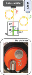 Experimental setup for FIFO-STM-NSOM-TERS
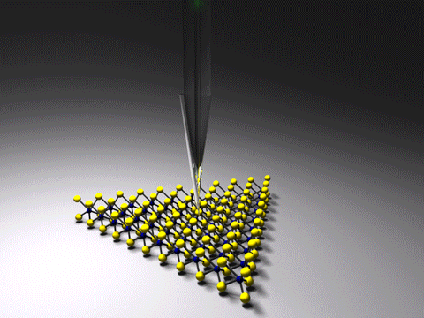
We develop a novel hybrid NSOM concept (Nature Photonics), which can be regarded as a combination of the merits from aperture- and apertureless-NSOM. Over all visible wavelength range, it can concentrate more than 50% of the incident light from an optical fiber to the tip of a silver nanowire (tip radius ~ 5 nm), for the study on light-matter interactions such as tip-enhanced Raman scattering (TERS, Wiki). The trick here is the selective excitation of the fundamental plasmon mode (TM0 mode). We have demonstrated the first fiber-in-fiber-out lens-free STM-NSOM-TERS by reforming an educational STM apparatus (NaioSTM), with which 1 nm spatial resolution TERS imaging has been proven on a single-walled carbon nanotube sample. We are working on the technique transfer to other NSOM platforms, including Horiba SmartSPM and Nanonics Multiview systems.
Nano UV-vis spectroscopic imaging
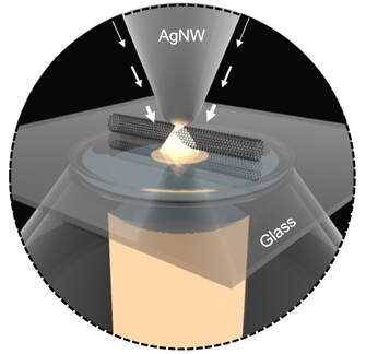 Conceptual image for Nano UV-VIS
Using the novel nanofocusing probe, we can improve the spatial resolution of UV-vis spectroscopic imaging from conventionally micron level to 6 nm (Nature Communication). To the best of our knowledge, this is the world record so far, ~ 5 times better than other reports. In this measurement, the "white" light from a tungsten lamp was nanofocused to the sharp tip of a probe to illuminate the sample from the near field. The scattered light contains information on the light-matter interaction at the nanometer scale. For the first time, we reported both the longitudinal and transverse excitons in single-walled carbon-nanotubes (SW-CNT). The strain-induced band structure variation in the SW-CNT was also reported. This technique is a powerful characterization tool for quantum science.
3D Scanning Photocurrent microscopy (3D-SPhcM)
The super-focused light source (~5nm in size, 1mW) can excite photocurrent in a semiconductor device, for the characterization of band-structure, doping, strain, photocurrent generation mechanism, etc. The manuscript is under preparation and more details to come.
NSOM for Quantum Science
We have developed a fabrication method to attach fluorescent nano-diamond particles to the tip apex of our probe. Due to the strong plasmonic enhancement effect and the large Purcell factor at the tip, the fluorescent intensity can be increased by about four orders of magnitude, making it an ultra-sensitive tool for weak magnetic fields. It can be used for nano-NMR or measure the magnetic field distribution in quantum materials.
Machine learning for Nano-photonics
 Machine learning for coupler designs
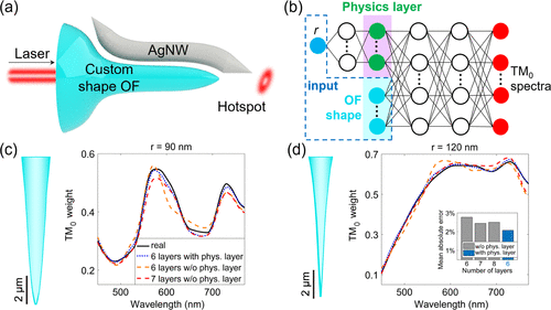
High-efficiency nanofocusing (~ 83%): The nanofocusing probe design in our first paper (Nature Photonics) used a simple conical geometry for the coupler. Although the nanofocusing efficiency was already revolutionary, there is still large room to improve. One solution is using axial-symmetrical probes with arbitrary profiles to elongate the coupling zone for the fundamental SPP mode and shorten the other regions. However, this optimization project requires a heavy simulation load if we sweep the parameters in traditional way. We develop a physics-guided two-stage machine learning network that uses the improved coupled-mode theory for optical waveguides to guide the learning module and improve the accuracy of predictive engines to 98.5%. A high coupling efficiency (83%) with symmetry-breaking selectivity is predicted by the inverse design. (More details in ACS Apply. Mater. Interfaces)
Machine-learning-assisted rapid nanoparticle size characterization: We have developed an optical technique using machine learning and a conventional optical microscope to predict the size of individual nanoparticles in the range of 80 nm to 200 nm, with an error of merely 5%. The paper is currently under review and more details will come soon. This technique can help to accelerate nanomaterial synthesis studies.
2D Material Optoelectronics
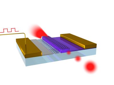 Graphene modulator
Modulators: 2D materials have remarkable electrical and optical properties. By integrating graphene with convientional silicon photonics, we have demonstrated the first graphene optical modulator. We are working on the next generation of 2D optoelectronic devices, in particular heterostructures, which have merits including deep sub-wavelength device size, low energy consumption, broad spectral bandwidth and high operation speed. We are also using the home-developed nanoscale photocurrent microscopy to investigate the carrier behavior near the electrode regions, which can help to develop novel electronics.
Nano-photodetectors: Along with the minimization of integrated photodetectors for on-chip optocommunication system, the different photoresponse mechanisms have their spatial distributions overlapped and, if not carefully designed, result in opposite polarities that cancel each other. The fully understanding of photocurrent generation mechanisms at the nanoscale was restricted by the diffraction limit of light. We develop a 3D scanning photocurrent microscopy (3D-SPhCM) to tackle this problem. The manuscript is currently under preparation.
Nano-photodetectors: Along with the minimization of integrated photodetectors for on-chip optocommunication system, the different photoresponse mechanisms have their spatial distributions overlapped and, if not carefully designed, result in opposite polarities that cancel each other. The fully understanding of photocurrent generation mechanisms at the nanoscale was restricted by the diffraction limit of light. We develop a 3D scanning photocurrent microscopy (3D-SPhCM) to tackle this problem. The manuscript is currently under preparation.
Modified PDMS-stamp transfer for 2D fabrication
Transferring 2D materials from the preparation substrates onto other substrates for functional heterostructure fabrication or simply for characterization plays an essential role in 2D material studies. A popular method for 2D material transfer is Poly(methyl methacrylate) (PMMA) transfer. In this method, PMMA solution is spin-coated on the 2D materials to form a thin supporting layer. Proper etchant solutions are then used to remove the original substrates and release the PMMA/2D material stack. The problem in this method comes from the long-chain PMMA molecules, which can not be fully removed from the material surface. Such residues not only influence the electrical performance of the transferred materials, but also make surface characterizations such as scanning tunneling microscopy (STM) imaging impossible. One alternative method is the 2D boron-nitride(BN)-flake transfer, where the BN flakes are used to pick up other 2D material(s) through the van der Waals adhesion. However, releasing the adhered 2D materials to expose their surfaces is impossible.
We improve the stamp-transfer method for clean 2D-material transferring. Due to the weak adhesion force between PDMS (polydimethylsiloxane) stamp and 2D monolayers, the conventional stamp transfer method cannot be employed on thin 2D materials. We increase the adhesion energy by utilizing the capillary force from a thin liquid layer (e.g. water) pre-condensed onto the PMDS film before stamping. In this way, the exceptional electrical properties of the 2D materials can be maintained after the water is evaporated. For example, a graphene-monolayer field-effect transistor (FET) fabricated on SiO2 has the carrier mobility of 48,820 cm2V-1s-1 at room temperature. Moreover, this method is very user-friendly, as it requires only some hot water for vapor and a soft stamp. If the 2D material is sensitive to water, other liquids (eg. ethanol) work as well.
For more details, please check our recent paper and two short videos:
Capillary-force-assisted clean-stamp transfer for two-dimensional materials, Nano Letters, 2017
video 1, video 2
We plan to improve this method for CVD graphene films on metal surfaces.
Plasmonics and Metamaterials
Surface plasmon polaritons -- electromagnetic excitations at metal-dielectric interface -- provides a novel way to concentrate light to enhance light-matter interactions. We reported the first nanoscale plasmonic actuator which generates large mechanical torque by changing the angular momentum of the incident light. More introduction can be found in Wiki. Currently, we are using our newly-developed NSOM to design novel plasmonic chiral structures.

This Fiber-in-fiber-out NSOM gif is licensed under a Creative Commons Attribution-ShareAlike 4.0 International License.
